The world of PCB assembly can feel like a complex maze, especially when it comes to testing.
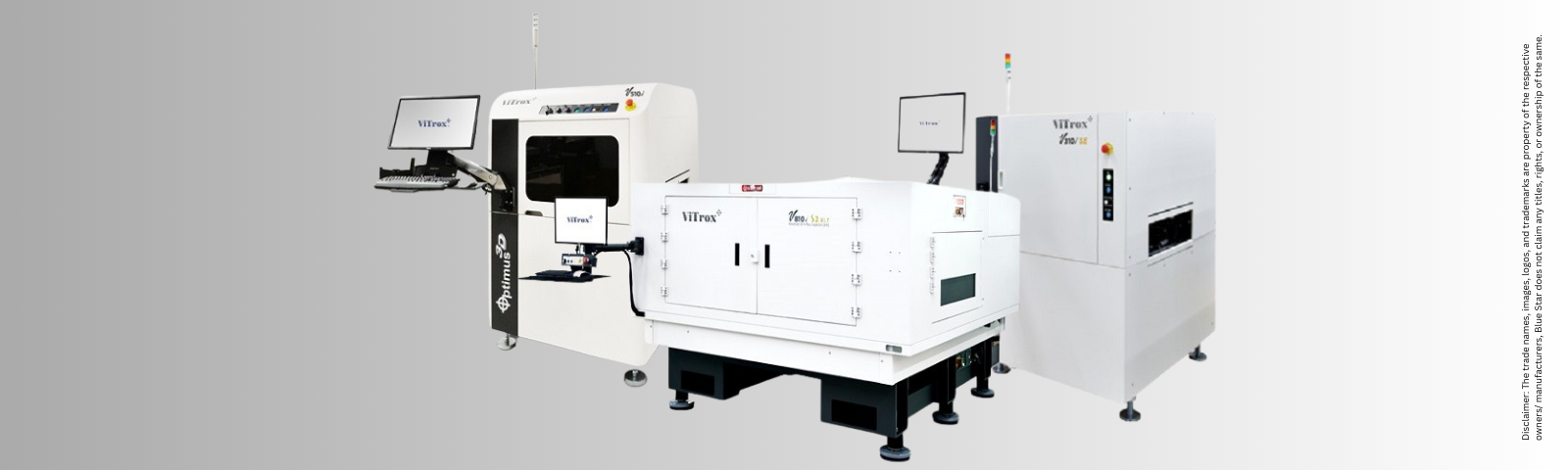
Ever wondered how PCBs are thoroughly checked for flawless performance? It’s all about a robust testing process, and key to that are these three important acronyms: AOI, AXI, and SPI. But what exactly do they mean?
Automated Optical Inspection or AOI –
Imagine a high-tech magnifying glass wielded by a tireless robot. That’s essentially AOI. It uses powerful cameras and image analysis software to meticulously inspect the surface of a bare PCB, before components are soldered on. AOI uses visible light and high-resolution cameras to capture images of the PCB (Printed Circuit Board) surface. These images are then analysed by specialized software to detect defects such as missing components, misaligned components, soldering defects, and other surface abnormalities.
Automated X-ray Inspection or AXI –
This technique goes beyond the surface, employing X-rays to see through the PCB and its components. AXI uses X-rays to inspect the internal features of a PCB, including solder joints, hidden connections under components, and internal structures. X-ray images are captured and analysed to identify defects such as insufficient solder, solder bridges, voids, and component misalignment that may not be visible to the naked eye or AOI systems.
Solder Paste Inspection or SPI –
In SPI (Solder Paste Inspection), cameras take close-up pictures of the solder paste applied to the PCB. SPI uses 3D imaging technology to measure the amount and quality of solder paste deposited on the PCB before component placement. Proper solder paste application is crucial for strong electrical connections, so SPI ensures a solid starting point for the assembly process. This ensures that the soldering is done accurately, which is important for the PCB to work properly.
Now that you know what each test does, the question becomes: which one do you need? The answer, like most things in life, is “it depends.”
Here’s a breakdown to help you navigate:
When it comes to basic surface inspection of components and solder paste, AOI is your go-to. It’s a cost-effective and efficient way to catch simple defects early on.
When internal flaws are a concern – AXI steps in. This is especially important for complex PCBs with tightly packed components or multi-layer designs.
And if one of the main objectives is ensuring a solid foundation for soldering: SPI takes the spotlight. This is vital for high-reliability applications where strong electrical connections are paramount.
The Synergistic Approach:
Often, the best course of action is to employ a combination of these techniques. Think of them as complementary tools in your PCB testing toolbox. AOI provides a quick and effective first line of defence, while AXI offers a deeper look for potential internal issues. Finally, SPI ensures a strong foundation for successful soldering.
By understanding AOI, AXI, and SPI, you’re well on your way to navigating the complexities of PCB testing. These powerful tools work together to identify and address defects early in the manufacturing process, leading to a higher quality, more reliable final product. So, the next time you encounter these acronyms, remember – they’re not roadblocks, but rather helpful signposts guiding you towards a flawlessly functioning PCB.
Elevate your PCB assembly and testing with the expert solutions from Blue Star E&E. Contact us to learn more now!
Our Solutions
About Us
Quick Links
Our Business
Connect with us