Bill Gates once said that “the advance of technology is based on making it fit in so that you don’t really even notice it, so it’s part of everyday life.” That statement resonates with the essence of Printed Circuit Boards (PCBs). Just as technology is seamlessly integrated into our daily lives, PCBs operate behind the scene, ensuring the smooth functioning of millions and billions of electronic devices around the world.
PCBs are at the core of almost all electronic devices we use today, from smartphones to medical equipment. But there are certain challenges to PCBs and therefore it is important to understand them so preventive measures can be taken.
Here are some of the more common challenges faced with PCBs.
These are gaps in the copper plating due to deposition issues and they tend to disrupt electrical currents in plated through-holes. Proper cleaning and adherence to manufacturing guidelines can prevent them.
Improper soldering, like cold soldering and contamination, can cause connection problems. Visual or X-ray inspections can identify these issues during assembly.
These copper or solder mask wedges result from manufacturing errors and can create unintended connections or corrode copper. Design checks and better manufacturing expertise can prevent them.
Using subpar components leads to damage during assembly, causing connection issues. Also, the miniaturization of components and circuitry is challenging for PCB manufacturers as smaller components require greater precision.
These come from design flaws. One needs to ensure that shielded cables and metallic packaging are used.
Moisture, dust, and temperature fluctuations can corrode PCBs, leading to failure. Proper protection shields boards from this
Components degrade over time, leading to leaks and breakdown. Regular checks and replacements extend PCB lifespan.
Maintaining quality across production is important as even minor defects can lead to malfunction.
PCB inspection and testing are crucial to manufacturing high-quality boards. Here are some of the inspection and testing services provided today.
The first step in PCB testing, here the boards are inspected for visible defects, such as soldering issues or physical damages.
Here cameras and algorithms are used to inspect PCBs for defects with high speed and accuracy. Missing components, soldering problems, etc. can be identified here.
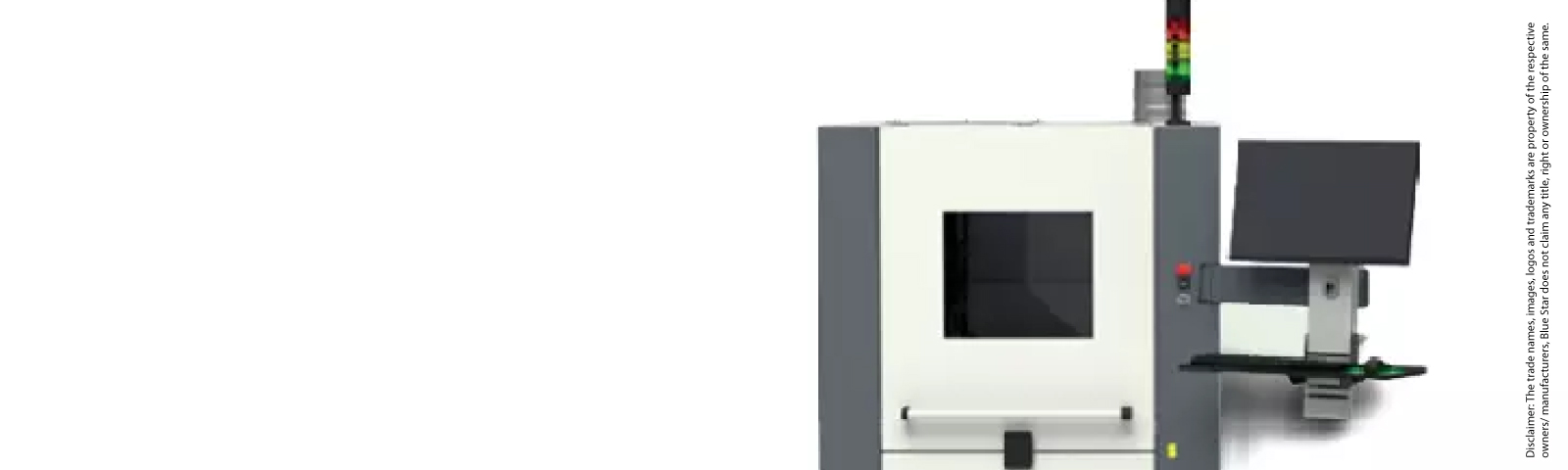
This is crucial for inspecting hidden solder joints and internal structures.
This involves testing individual components and connections such as open circuits on the PCB to identify defects and faults.
Here, the PCB’s performance is assessed by evaluating the PCB’s response to different inputs to see if it produces the expected outputs.
PCBs are subjected to environmental conditions such as humidity and vibration to determine their reliability under different stressors.
PCB manufacturing is a complex and challenging process and therefore inspection and testing services are extremely important to identify and rectify defects. Blue Star E&E’s PCB testing solutions are designed to ensure functionality, reliability and quality. And to guarantee optimum performance. Give our experts a call today.
Our Solutions
About Us
Quick Links
Our Business
Connect with us